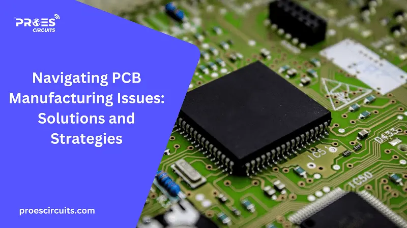
Introduction
However, the journey from concept to fully functional PCB is fraught with potential pitfalls. PCB manufacturing issues can emerge at any stage of the process, from design to assembly, threatening to compromise the functionality and reliability of these critical components. These challenges range from soldering defects and etching errors to component misalignment and inadequate copper plating. Each issue, if not promptly identified and addressed, can lead to significant setbacks, including increased costs, delayed product launches, and, most critically, diminished device performance.
The intricacy of modern PCBs, coupled with the demand for rapid production cycles, exacerbates the potential for manufacturing errors. As PCBs become smaller, with more components packed into tighter spaces, the margin for error diminishes. This evolution makes the identification and resolution of manufacturing issues not just a matter of quality control but a fundamental aspect of the manufacturing process. Ensuring the production of high-quality, reliable PCBs necessitates a comprehensive understanding of common manufacturing challenges and the implementation of robust troubleshooting strategies. Recognizing and mitigating these issues early in the manufacturing process can significantly enhance the performance and reliability of electronic devices, underscoring the critical importance of diligent PCB manufacturing practices.
Understanding PCB Manufacturing Issues
The PCB manufacturing process is a complex, multi-stage endeavor that requires precision and expertise at every step to ensure the production of functional and reliable boards. This process begins with the design phase, where circuit layouts are meticulously planned and laid out using specialized software. Here, attention to detail is crucial, as even minor oversights can result in significant issues down the line. Following design, the process moves to printing, where the design is transferred onto a copper-clad laminate. This step sets the stage for etching, where unwanted copper is removed to reveal the circuit paths. Any inaccuracies in this phase can lead to broken or incomplete circuits, severely impacting the board’s functionality.
Assembly is the final stage, where electronic components are mounted onto the PCB. This phase involves precise soldering and placement techniques to ensure that each component is securely attached and correctly connected. Faults during assembly can lead to short circuits, open circuits, or misaligned components, all of which compromise the board’s performance.
Each stage of the PCB manufacturing process, from design to assembly, is intertwined and critical. Faults at any phase can cascade, magnifying the impact on the final product. Hence, it’s imperative that both the design and manufacturing teams exercise meticulous care and attention to detail throughout the process. This vigilance helps to minimize errors and avoid the common issues that can otherwise undermine the quality and reliability of PCBs.
Common PCB Manufacturing Issues
Soldering Defects
Soldering defects are among the most common issues in PCB manufacturing, significantly impacting board functionality. Cold solder joints occur when the solder does not melt completely, leading to a weak bond between the component and the board. This can result in intermittent connections or complete failure of the circuit. Solder bridges, another common defect, happen when excess solder forms a connection between adjacent pins or pads that should not be connected, potentially causing short circuits. Both of these defects compromise the reliability of the PCB and can lead to device malfunctions.
Etching Errors
Etching is a critical step in PCB manufacturing, where chemical solutions are used to remove unwanted copper, leaving behind the desired circuit paths. Errors in this process, such as under-etching and over-etching, can have detrimental effects. Under-etching leaves excess copper on the board, which can create unintended connections between circuit elements. Over-etching, on the other hand, removes too much copper, leading to broken or incomplete circuit paths. Both errors disrupt the intended functionality of the PCB, affecting the overall performance of the electronic device.
Component Misalignment
Component misalignment occurs when parts are not placed correctly on their designated pads or when orientation is incorrect. This misplacement can lead to malfunctioning circuits, as the electrical connections required for proper component function are not correctly established. Misaligned components can also complicate or prevent further assembly processes, impacting the manufacturing timeline and increasing costs.
Inadequate Copper Plating
Copper plating on via and pads ensures robust electrical connections between PCB layers and components. Inadequate copper plating can result in weak connections, making the PCB susceptible to breakage and failure, especially under conditions of high current or mechanical stress. Furthermore, insufficient plating can lead to the development of short circuits, as the thin layer of copper might not withstand the electrical load, causing overheating and potential damage to the board and connected components.
Troubleshooting Techniques
Visual Inspection
A thorough visual inspection remains a cornerstone of PCB troubleshooting, serving as a first line of defense against manufacturing defects. Skilled technicians can spot a variety of issues, including soldering defects, component misalignments, and etching errors. This method is cost-effective and immediate, allowing for quick identification and correction of obvious flaws before moving on to more sophisticated inspection techniques.
Automated Optical Inspection (AOI)
Automated Optical Inspection (AOI) systems leverage advanced cameras and software to scrutinize PCBs for a wide array of defects that might escape the human eye, such as minute soldering errors or slight component shifts. AOI can rapidly inspect boards in great detail, making it an invaluable tool for ensuring high-quality production in high-volume manufacturing environments.
Functional Testing
Functional testing involves powering up the PCB and verifying its operation against the expected outcomes. This crucial step ensures that the board performs its intended function correctly. By simulating the real-world conditions in which the PCB will operate, functional testing can uncover operational issues, including those that may not be visible, such as incorrect component values or subtle logic errors.
X-ray Inspection
X-ray inspection provides a deeper look into PCBs, allowing technicians to view layers and components obscured by other parts. This technique is particularly useful for identifying soldering defects underneath components, such as BGAs (Ball Grid Arrays), where visual inspection is not possible. X-ray inspection can reveal issues like solder voids and bridge connections, offering a comprehensive assessment of solder quality and component alignment.
Preventive Measures and Best Practices
Emphasizing preventive measures is key to minimizing PCB manufacturing issues. Proper design validation, including thorough pre-production simulations and checks, ensures that potential problems are identified early. Implementing rigorous quality control checks at each stage of manufacturing, from component placement to final assembly, helps catch and correct errors before they escalate. Adherence to industry standards guarantees that manufacturing processes meet the highest quality and safety benchmarks. Establishing a routine review process for continuous improvement and investing in ongoing training for the manufacturing team ensures they are well-versed in the latest technologies and methods. These practices not only prevent common manufacturing issues but also foster a culture of quality and excellence.
Conclusion
The role of troubleshooting in PCB manufacturing cannot be overstated. Identifying and addressing common manufacturing issues is crucial for ensuring that PCBs meet the high standards required for functionality and reliability in today’s technology-driven world. Implementing the discussed troubleshooting techniques and preventive measures is essential for minimizing defects and enhancing the overall quality of PCB production. Manufacturers that proactively seek to understand and mitigate these issues will find themselves at the forefront of the industry, producing PCBs that are not only high in quality but also reliable and efficient. It is through such diligence and commitment to excellence that the future of PCB manufacturing will continue to evolve and improve.